In order to solve the long time problems plaguing my attempts at creating fast switching high power electronics circuits, I’ve decided to take a crack at simulating it using ngspice.
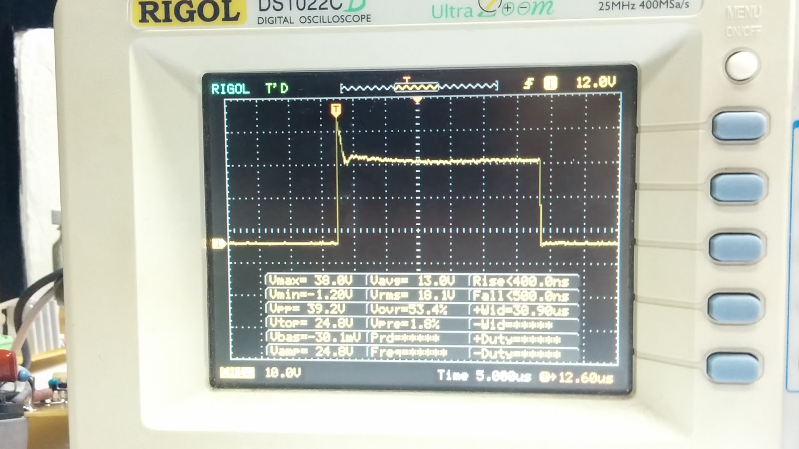
Here is a view of the kinds of ringing I am getting whenever the FET opens at load:
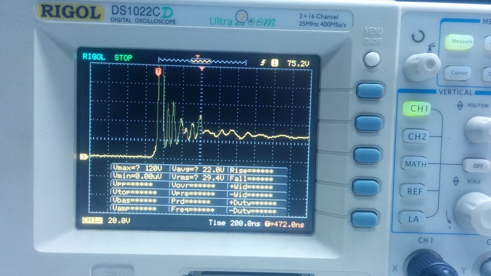
The very large spike (too large to measure on this probe but greater then 120V according to Vmax in upper left) and high frequency ringing (8MHz) cause serious problems all around the circuit. For example the microcontroller keeps resetting itself, and after investigation, there is about a 1.5V 8MHz transient across the ground wire leading to the microcontroller! This is just across the wire. So there is clearly something very wrong in this circuit.
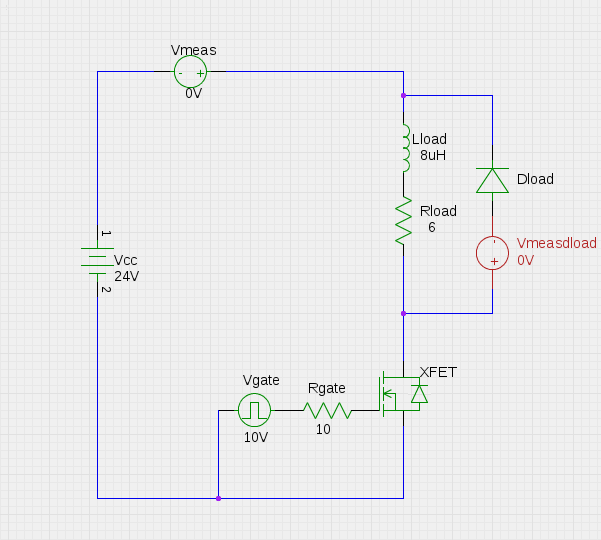
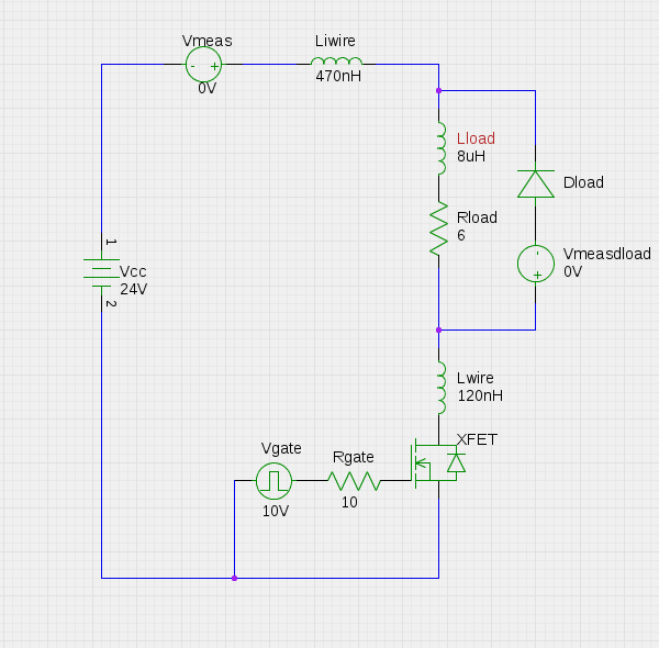
Therefore, to begin, here is the basic schematic of the circuit:
The first main discovery (that pommm pointed out to me! thanks pommm!) is that many vendors publish spice models of their parts on the internet. In particular, the FET and high speed diode should be modeled reasonably closely in order to try to get the ringing effects that are so problematic in the simulator. Here is a link to the IRFP250N FET and RFN60TS6D diode spice models that I am using for this test. (Actually, that isn’t the exact model of diode we are using, and we changed the FET around a bit with the IRFP250N only one of the FET’s we tried, but it is similar enough. The problems we saw were pretty much the same on all the real components we tried.)
Here is the resulting plot of the simulation of this simple idealized model of the circuit using ngspice:
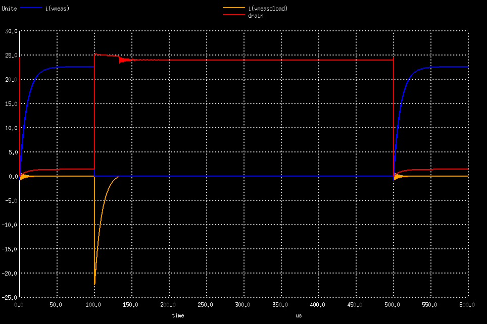
In red is the voltage across drain-source of the FET, in blue is the current from Vin, and in yellow is the current passing through the freewheeling diode Dload (negated to make it easier to see in later plots). You can see the FET closing at the beginning (red plot) followed by a rise in the current from Vin (blue) until the FET opens again (red plot around 100us) followed by the freewheeling diode taking up the current in the load inductor until it dissipates (yellow plot from 100us to about 130us). In particular, note that there are no significant voltage spikes across the FET at 100us. (The ringing on the red plot after the diode current drops to zero is probably some kind of oscillation caused by the diode forward voltage preventing it from fulling dissipating the power in the inductor, but this is acceptably small.)
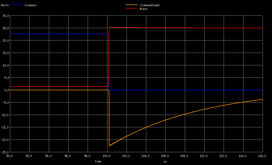
For reference, here is a zoomed in version from 90us to 115us to see what is happening when the FET opens:
This graph doesn’t correctly show the problems we are seeing in the actual circuit, so we know we need to add some more characteristics of the real circuit not accurately represented in the simulation. Since voltage spikes that occur when a switch opens are likely caused by some kind of inductance, and we have modeled all of the intentional inductor components in our circuit, this suggests we need to start modeling the parasitic inductances that are caused by the various power wires along this path.
The idea here is that the inductance <-> voltage relationship is governed by the equation
V = L dI/dt
Even though L on a wire is something tiny like 100nH, dI is about 25A and dt is about 15ns, resulting in a voltage spike of about 170V in this example.
So I chose to model the inductance of the wire between the battery and the load in addition to the inductance of the wire between the load and the FET. I chose the values of 470nH and 120nH respectively by looking up the inductance of the large gauge copper wire I am using at about 30cm (battery->load/diode junction) and about 8cm (load/diode junction to FET).
Now the schematic looks like this:
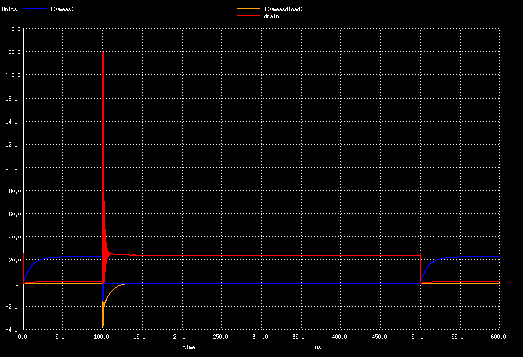
And here is what the simulation looks like now:
And zoomed in on 90us to 115us:
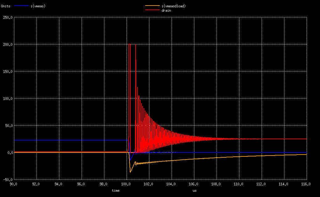
Notice the 200V spike followed by very high frequency ringing for about another 10us. Now this is a reasonable approximation of the problem we are seeing in the real circuit. And since the FETs we are using have max voltage ratings between 100V and 200V, this spike clearly has the potential to cause problems.
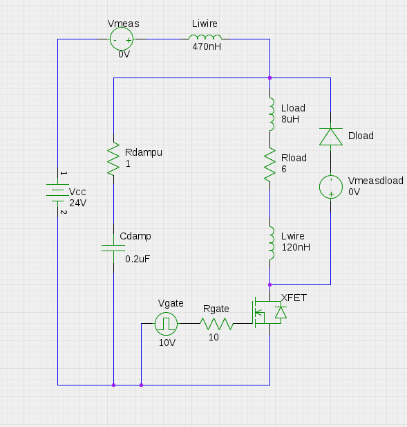
After playing with different combinations of options, I was able to fix the problems associated with the parasitic inductance on the wire between the load connector and FET by “extending” the diode Dload so that it “covers” this wire too. In reality, we would just want to eliminate it entirely by moving these points on the circuit closer together as much as possible. The other issue (input wire inductance) was a bit more tricky since the wire between the power source (batteries) and the circuit can’t be spanned by a diode on the circuit board. So instead I played with different combinations of R-C filters in the simulation to try to introduce a capacitor that can soften some of the built up voltage spike from the wire inductance once the switch (FET) opens.
As a metaphor, I liken this to a steel toolbox being shaken quite violently side-to-side. (Switching large currents on an off is a little like shaking stuff.) If you have a hammer inside, it will start to bang against the sides quite powerfully causing loud ringing. In this case, you can’t soften the shaking since slower shaking (i.e. slower switching) would result in too much heat buildup in the FET. The best you can do is put a little bit of padding inside the box so that the impacts are not so violent as to cause ringing.
Here is the circuit I ended up with:
And here is the new simulated plot:
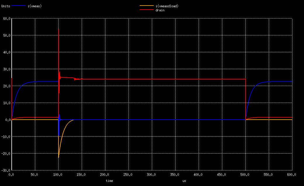
First, notice that the voltage spike has dropped from about 200V to less than 55V. This is well within the specs of the FET.
Next, take a look at the zoomed in plot:
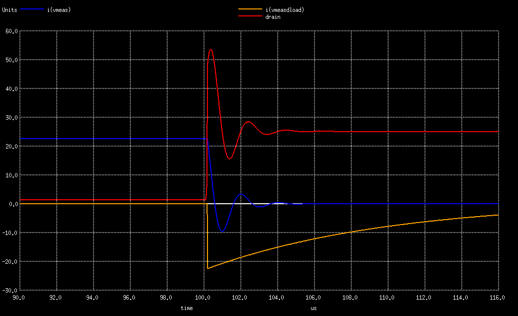
The ringing has reduced to just one significant period and one more tiny ripple. This is a dramatic improvement on the original.
For the record, here is the ngspice netlist I used:
switching inductor test
*
.INCLUDE lib/irfp250n.lib
.INCLUDE lib/rfn60ts6d.lib
.tran 5ns 600us
vin vcc gnd 24v
vmeas vcc omeas 0v
lmotor top midload 10uH
rmotor midload iwire 1
xfet drain gate gnd irfp250n
vgate pulse gnd PULSE( 0V 15V 15ns 1ns 1ns 100us 500us )
rgate gate pulse 10
dload midloadl top DRFN60TS6D
vmeasdload midloadl drain 0V
lwire iwire drain 120nH
liwire omeas top 470nH
rdampu top updamp 1
cdamp updamp gnd 0.2uF
.end
Updated 2015-12-14: Fixed direction of diode across FET in schematic drawing. Problem was only in the drawing, not in the circuit. 🙂